Wednesday, March 21, 2007

Cenamps on YouTube: Stimulating Innovation and New Ventures

Sunday, March 11, 2007

Microsoft has visions of bringing the Internet straight to your Wallpaper

Whilst Google has visions of bringing a network smart billboards to a shopping centre near you, Microsoft has visions of bringing wide-screen displays that integrate into our everyday lives just like wallpaper.

As digital technologies shapes and flattens the 21st century economy and consumers increasingly embrace the Internet and smarter products, only the high cost of installing unobtrusive displays technology is stopping this from happening today.

Whilst there are greater choices today in emerging display technology, each technology has a drawback. For example, front projection displays have the problem of shadows cast. Rear projection displays take up floor space—one of our most precious resources. LCDs, although a mature technology, require expensive manufacturing processes.

Microsoft believe that whilst some of these problems have been addressed in the lab, the costs of manufacturing displays for the consumer market has yet to be solved. Microsoft are hence exploring ways to build low-cost miniature display cubes that could be tilted together to form any size display. The technology behind this is called MicroElectoMechanical Systems, or MEMS.

Although most of Microsoft's developments are in software, Microsoft Research has indicated that its hardware devices group is currently building micro-devices using MEMS in an effort to build cheaper flat-panel displays with high resolution. "We want displays to become as unobtrusive as wallpaper" the research team says on their Web site.

The group is set to demo their research this week at TechFest 2007.

Just imagine an array of tiny machines, each the size of a human hair or even smaller, spread across the walls of your Smart Home. They could be tilted to display say an image or movie of your choice or tilted to form a computer screen of any seize on your wall - bring a new dimension to home entertainment.

MEMS technology is currently picking up steam for use in of entertainment products, including Nintendo's immensely popular Wii gaming console.

Flexible organic displays offer yet another alternative low cost technology. This is an areas Cenamps is driving with the build of the Polymer Electronic Technology Centre (PETeC) planned to start shortly in Netpark, County Durham.

Shak Gohir

Labels: , ,

Wednesday, February 14, 2007

Google Hints at Smart Billboards & Digital Display Networks for Advertising in Malls, Hotels, ATMs, Shopping Centres and Outdoors

Google may start appearing on digital billboards and displays in a shopping centre near you. The company recently filed a patent application for technology that will allow local stores to connect their stock control systems to a Google-powered network of electronic displays.

The patent, filed December 21, 2006 with the United States Patent and Trademark Office, covers systems and methods for allocating advertising space in a “network of electronic display devices.”

"Advertisers may upload advertisement messages to a server specifying information such as budget, price per impression, preferred billboards and other constraints. One or more keywords or other descriptors are specified for each advertisement message,” according to the filing.

Google's system would then generate an advertising campaign specifying where on the display devices the advertisement message will appear. “The output may consist of various forms, including video, audio, printed incentive, interactive data transfers and/or combinations of these,” the company mentioned in its filing.

If the filing is a sign of things to come from Google, kiosk billboards, ATM machines and other digital displays in shopping centres and hotel lobbies could start promoting products and services directly from a nearby retailer’s inventory and/or service offering. Presently, advertising via similar screens is limited to looped, poster-type advertisements, in Google’s vision, the ads could be pulled directly from a retailer’s stock control system.

In the filed patent application, Google explained that its technology could remove the burden of manually loading looped ads, instead enable retailers to create campaigns from available goods. The adverts can be displayed in rotation and stopped automatically once the product has sold out. Once the product is back in stock, the advertisement can be re-added to the display cycle.

Shak Gohir

Labels: ,

Tuesday, December 26, 2006

The Opensource Handbook of Nanoscience and Nanotechnology

The Opensource Handbook of Nanoscience and Nanotechnology is a wikibook on nanoscience and nanotechnology gathers information about the various tools, methods and systems to provide students, researchers and everyone else an open-source handbook and overview guide to this vast interdisciplinary and expanding field - a book that can be adjusted as new things appear and improved by its readers.

You may also be interested in reading the section on "Nanotechnology" in Wikipedia.

Shak Gohir

Labels: ,

Tuesday, August 08, 2006

Googling for nanotechnology


Who is googling the world wide web for nanotechnologies?

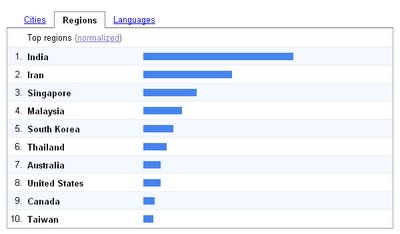
This is a question that I put to Google Trends. When I tapped in the word "nanotechnology" into Google Trends during the afternoon of 8th August 2006. I was surprised by the answer. The answer that Google Trends threw out was India - it was not China, Europe, South Korea, US or Japan. What is more, people in India are googling for online nanotechnology content at a level that significantly exceeds any other nations.


Google Trend also indicates that the top language in which "nanotechnology" is searched for is Korean and not English. So India and the rest of the world must be searching South Korean websites for nano content more than sites from other regions and nations?
This is not to say that today India is a leading player in the nano field. As it happens, India is a late starter when it comes to nanosciences and nanotechnologies and still needs to build critical mass. India started its Nano Science and Technology Initiative just five years ago, during 2001, and has invested just around $24 million to date.

What it does indicate is the increasing inner passion of individuals studying and/or working in India to strengthen their nation's global economic position through high-tech R&D and not just services and information technology.

An article published recently during June 2006 by the Science & Development Network "
Preparing for take-off: Indian nanotechnology" says:

".... Brij Mohan Arora, a materials scientist at the Tata Institute of Fundamental Research in Mumbai points out that, overall, India does not have many achievements to showcase yet. "Much of it has been small table top research, but nevertheless it has created an awareness about techniques," he says.

If India wants to catch up with the best of the world's nanoscience researchers, and apply the technology to developing world issues — such as energy, water and health care — it seems that far greater investment is needed.

Fortunately for India, it is one of the few countries whose leader is pushing to improve funding for the sector. President A. P. J. Abdul Kalam, a former scientist in the space and defence sectors, was one of the first to point out that the country's nanotechnology research was sub-optimal.

In April 2004, Kalam organised a meeting of nanoscience experts to devise a national mission plan. Its recommendations include spending US$22 million each year for the next five years on five new national facilities specialising in complimentary areas of nanotechnology and ten 'mini centres' across the country. These centres would each receive US$5 million, and would focus on one or two areas of nanoscience and technology.

Overall, the experts recommended that US$200 million be spent on nanotechnology over a five-year period. India's finance ministry has now cleared these funds for use in 2006-2011. From later this year, the new national mission will oversee activities currently under the Nano Science and Technology Initiative.... "

Setting aside nanotechnology for a moment, a survey conducted by INSEAD and Booz Allen Hamilton, indicates that R&D is moving east. It suggestions that by the end of 2007, India and China will account for over 30% of global R&D staff, up from 19% during 2004.

Shak Gohir
Business & Programme Manager

Labels: ,